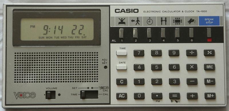
This rare gadget of 1983 (?, concluded from Microdigest advert scan) is the only talking calculator made by Casio. Additionally it has a schedule alarm clock with 6 alarms, each announced by a (pre-programmed) corresponding word (only No. 6 is a grainy dog bark).
Unlike Sharp calculators it can only speak ciphers but no complete numbers. The synthetic female voice has a similar grainy timbre like TI - Speak & Spell and resembles that of Sega's mythical arcade game Zektor. Particularly the additional 'cuckoo' (time signal) and 'dog bark' (alarm 6) sound heavily synthesized.
Unlike calculation results, the numbers of time and date are spoken properly (not cipher by cipher) by pressing their button. E.g. "time" says "eleven fity-nine AM", or "date" says "wednesday june twenty-seven", i.e. the speech synth can pronounce numbers up to 59 (not used by calculator) and the names of days and months.
In 'set' mode pressing "AC" and then the "speak" button speaks out time and date followed by all 6 alarm messages and their on/off state, which may be considered a kind of demo.
The "=" button cycles the hourly time signal through 'gong', 'cuckoo' and off while sounding the selected signal.alarm-1: "It's time to wake up." (twice) alarm-2: "It's time to go out." alarm-3: "It's time now." alarm-4: "It's time for your appointment." alarm-5: "It's time for the meeting." alarm-6: "Bow-wow" (= dog bark, 4 times)
The calendar is Y2K compliant (years 1901 to 2099), but unlike in most
Casio calculators, the date is set here without pressing "date" in between.
While dates up to 1999 were 6-digit numbers (format "yymmdd"), since 2000
it has to be entered as 8 digits (format "yyyymmdd") followed by "adj-set"
(push with thin object). E.g. "20010215" results in "2001-02-15" for 15th
February of 2001. Typing 3 or 4 digits (with optional 'PM' button) the
same way sets the time. It has no date calculation.
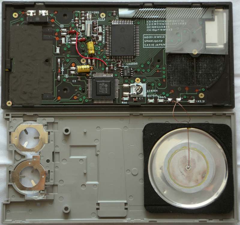
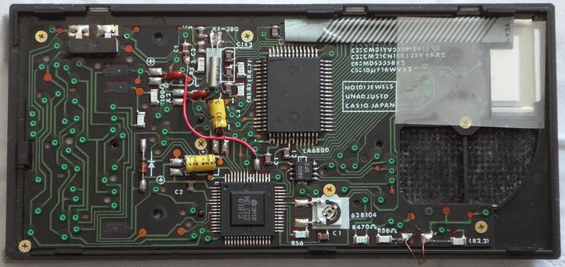
circuit bending detailsThe Casio TA-1000 is based on an unknown version of the D1864G CPU (soldered upside-down, crystal clocked likely at 32.768 kHz), which communicates with an additional speech IC "HD61912 C02" (with resistor controlled clock oscillator). Both route their sound through an amp IC to the piezo speaker.
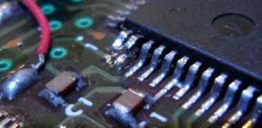
caution: The LCD foil cable is fragile. Never pull at it (it may snap off) nor sharply fold it (carbon traces crumble off). Handle it with extreme care. (If the cable comes loose at an end, install an adhesive foam rubber strip to press it on.) Do not remove the PCB or LCD if avoidable. Particularly avoid to remove the transparent adhesive behind the display, which may damage the foil cable. Fortunately the stabilizing black adhesive film on the opposing side of the connector is a separate piece. So with some care I could safely peel of the rest of the black foil that covers the back of the battery compartment to examine the PCB underneath. While the CPU runs on a single battery, the speech IC needs an additional negative voltage, hence a 2nd battery. Both lithium batteries are wired in series with center tap. The upper +3V battery is connected with its plus pole to the positive supply voltage of the CPU; the minus pole (center tap) goes through a 100 Ohm resistor to the ground 0V pin of both CPU and speech IC. The lower -3V battery has its minus pole wired to the -3V negative supply voltage input of the speech IC. Additionally a polarity protection diode goes from there to ground 0V; it may be there to prevent chip destruction by upside-down battery insertion, but may also prevent charging wrongways if one is full and the other empty because, that is to say, such lithium batteries are also reported to detonate with the vigour of shotgun shells if accidentally charged. The reset pin of the CPU is active-lo but of speech IC is active-hi. Therefore the reset switch has 2 contacts to pull CPU pin 62 to 0V (from battery through a separate 100 Ohm resistor) and speech IC pin 50 to +3V. With opened case it is mechanically difficult to connect batteries. Through test leads +3V can be fed to the right metal pin and 0V (through a 100 Ohm safety resistor) to the left metal pin of the reset switch (or upper pin of the diode). -3V can be fed to the lower pin of the diode. (I used an external battery compartment with 4 AA cells instead of messing with those lithium firebombs.) pitch control ? shitshot The clock frequency (independent from host CPU) is set by a 10k trimmer (in series with 56k resistor) from speech IC pin 39 to 40, which sets pitch and speed of the speech. My trimmer was broken (damaged carbon trace to center pin), so I soldered a very thin wire from the center rivet at its back to the lower pin to make it work. The clock signal is also output on pin 8 (buffered, roughly 132 kHz) and 9 (unbuffered, different phase?); shorting both or touching 9 e.g. with oscilloscope probe makes strange loud crash noises, those can be semi-metallic or modem-like. They sometimes make freakish glitch nonsense like in Speak ? Spell, but this happens less often and the sound character differs. So I am not sure if the speech synthesis engine is really LPC based (buzz + hiss + resonance filter = simulated vocal tract) or only a kind of wavetable synthesis. But the unnatural grainy effect sounds {dog bark, cuckoo, gong} suggest that it was not optimized to faithfully reproduce other things. Also touching the quartz of the main CPU or shorting both pins can produce the infamous R2D2 glitch. Reset the CPU to exit. test modes
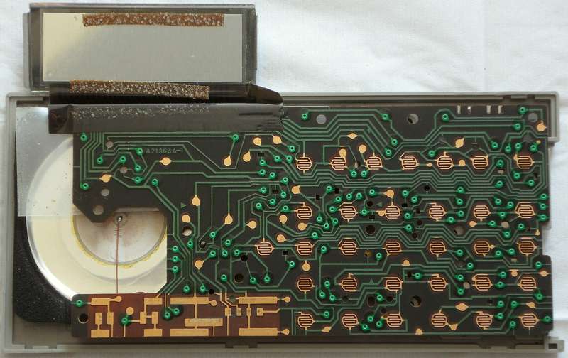
Pulling pin 63 hi enters another test mode which adds glitches to the display contents. The '5' key sounds a continuous tone with random(?) pitch (and previous volume step?). Pressing again makes the volume increase by each one step (7 in total) and return to 0 (silence), which was likely made for DAC testing. This is interesting because (unlike related musical calculators) the TA-1000 CPU normally only plays blip and alarm tones of fixed volume (no envelope). Key '4' (sometimes also '0') sometimes switches pitch 1 note up. (I haven't checked for test data on matrix pins.) keyboard matrixThe keyboard matrix has no diodes and is multiplexed with the speech IC. The only 4 input lines hint to a simple 4-bit architecture. The layout of columns 10 and 11 partially resemble ML-90. I found no eastereggs.
The input lines are active-high, i.e. react on +Vs. Any functions can be triggered by a non- locking switch in series to a diode from one "out" to one "in" pin. In idle mode the matrix out pulses have only 2Hz, despite inputs are
sensed faster. Likely it does an additional pulse when input voltage changes.
The slide switch needs no locking contacts.
The speech IC is controlled by a simple protocol using 3 of the matrix pins. The CPU outputs sync pulses on pin 17. To speak a word, it outputs the corresponding word number as serial data on pin 18. While it is speaking, the speech IC sends a busy signal by pulling CPU pin 8 hi during the sync pulses from pin 17; by this handshake the CPU knows the correct timing to start the next word only after the previous is finished. (All words are stored in rom of the speech IC, can have different lengths, and their duration also depends on the pitch trimmer setting.) Despite CPU pin 6 is also wired to speech IC pins 15 and 31, these are NC (internally not connected) and only used to route the trace further to other keys.) The amp IC "6800" (PCB label "LA6800")
could not be identified. I suspected relation to the precision op-amp "Linear
Technology LTC6800" (also 8 pin SMD) but the pinout differs.
pinout LA6800The "6800 3F2" is is a small bridged audio amplifier IC (8 pin SMD) found in Casio TA-1000, on which PCB it is marked "LA6800" ("LA" = linear amplifier?). It seems to be a sort of op-amp (possibly specialized for) driving a piezo speaker, but I found no info about it.The pinout is not related to the precision op-amp "Linear Technology
LTC6800". All pin names were chosen by me.
The way it installed, the output is clipping the peaks of the speech signal, which is likely caused by the limited supply voltage in combination with the piezo speaker. I haven't examined this IC in detail, so e.g. signal polarity may be wrong. In normal operation the audio inputs 6 and 7 have 0V DC and 5 (negative supply voltage?) has -2.9V. But during standby pin 5 raises to +2.4V (likely turns amp off) and also pins 6, 7 raise to +2.9V (hi level of the speech IC). For test I pulled each pin hi (to +3V) through an 1uF cap: 3 => dull, low volume
pinout HD61912The "Hitachi HD61912 xxx" (60 pin SMD, pins count anticlockwise, xxx = software number of internal rom) is the speech synthesizer IC of the talking calculator Casio TA-1000 (software number "C02"). It has an internal DAC (likely 12-bit) and communicates with a host CPU through a simple 3 wire protocol (serial data + handshake) to output individual words or sounds from its internal rom.The stored sounds are heavily data-reduced; this synth engine makes bizarre distorted loud glitch noises during crash (e.g. modem-like or semi-metallic). I am not sure what it is exactly, but the Hitachi patent US4435832 (Japanese priority date 1979) about speech synthesis with time stretch and compression function (i.e. dynamically changeable playback speed) may be related to it, which describes a PARCOR based LPC algorithm. The IC is actually printed "Hitachi, 3M13, HD C02, 61912" (rows top-down), but from HD61914 (seen in other calculator service manuals) I learned how to interpret this letter mess correctly. This obscure chip has way more pins than necessary for this application, despite no other talking Casio calculators are known. Interesting is that the pocket computer Casio PB-100 (aka Radio Shack PC-4) of 1982 contains a CPU "HD61913" (80 pin SMD, seen in PC-4 service manual) with 2x SRAM HD61914, which may help to estimate age and hardware platform it was designed for. (Important: By lack of schematics, all pin names were chosen
by me, an will change if I ever find schematics.)
This obscure synth chip has a large number of unused pins and was likely designed for something else, therefore I tried hard to examine deeper what it does, because it is such strange. Possibly it even can be hacked to read sound data from an external rom (see pin 35), although soldering these tiny pins is nothing for the fainthearted. The specs of HD61912 would nicely match the ADPCM speech IC "OKI MSM6212GS" (60 pin SMD, 3V supply, clock rate 32768 kHz (30..132kHz), 2 pin audio out) however the pinout strongly differs, so it might be an unofficial predecessor. As a Hitachi chip it also might be a special variant of HD38880 with internal speech rom. The IC needs positive and negative supply voltage and goes into standby (auto-power-off) after about 24s (depends on clock trimmer setting), which also disables data on test pins. The logic level hi=+3V, lo=0V (not -3V). The clock frequency (independent from host CPU) is set by a 10k trimmer (in series with 56k resistor) from pin 39 to 40, which sets pitch and speed of the speech. 39 shows a triangular wave, while 40 has a more jagged waveform (tri mixed with square?) at lower level, that reduces pitch stronger when touched, hence I conclude that 39 is output and 40 is input. My trimmer was broken (carbon trace to center pin), so clock rate was way too low. The clock signal is output on pin 8 (buffered) and 9 (unbuffered, different phase?) shorting both or touching 9 with oscilloscope probe makes strange loud crash noises. On my analogue scope the buffered clock frequency looks like roughly 132 kHz. Audio is output through pins 43 and 47 to the amp IC; pin 44 outputs -2.9V to supply it; in standby this pin goes hi (+2.4V) to turn the amp off. Pin 38 seems to be some kind of feedback signal from an amp output. The amp outputs have clipping distortion, thus undistorted audio should be taken from speech IC pin 47. Pins 15, 31, 46 are NC. Despite they are wired to other pins, when desoldered they are completely high resistance (have neither reverse diode nor change oscilloscope hum waveform), hence they are internally not connected. Pins 4, 5, 6, 56 seem to be internal reference voltages (stabilized by external capacitors). Pin 5=0.65V (>0.85V during speech); pulling hi though 1k resistor makes pitch lower, though 330 Ohm crashes, pulling lo does nothing. Pin 6=0.37V (0.47V during speech). Pin 6=-2.89V. Pins 16..27 seem to output 12 individual DAC bits. Pins {28, 30, 32, 33, 34} output each a multipulse (bit loop, about 20 steps?) that rapidly changes during speech but stays constant during silence. These may be test pins showing internal register contents. Pins 51..53 are wired to 0V. If desoldered and pulled hi, they make strange unspectacular crashes. Touching any of them with a probe at hi level makes the chip ignore inputs (sometimes finishes the currently spoken word and then stops?) until all pins were touched with lo (0V) again. Likely these are simply inverted "chip select" inputs, those turn all inputs off if any of them is pulled hi, and it is internal capacitance that made it store that voltage level for a while until all get touched with "lo" again. The unused pins {2, 3, 7, 10..14, 29, 36, 48, 49} normally stay always either hi or lo (depending on the pin). But most exciting is pin 35; like 36 it is wired to +Vs, but when desoldered and pulled lo, it causes wicked crash noises and many of these normally unused pins come to life and output data (or frequencies?). Sometimes also 35 or 36 (normally lo) have hi level after that. With 35 open, the chip gets very hum sensitive (can crash or output buzz by finger on the plastic package) and those unused pins sometimes show waveforms with intermediate voltage levels (digital signals mixed with analogue hum?, seen on analogue scope). Likely 35 is the test mode enable pin. But it would not surprise me if it even can disables the internal speech rom to make the chip read synth data from an external data bus. I soldered it back to avoid hum sensitivity. The resulting crash noises were very similar like those of messing with clock pin 9, which is much safer to access, so I soldered it back on. (For circuit bending it would be sufficient and safer to mod only the pitch trimmer and install shitshot controls on clock pin 9 (which already has its own test pad on PCB), so stay away from pin 35 if you don't need to.) Also pin 1 is likely a test mode enable pin. Despite positive supply voltage is typical for pin 1, here it makes little sense since there are already 2 other groups of {+3V, 0V, -3V}, so why should there be another +Vs? When desoldered, the pin is hi but speech pitch sounds a little lower and about every 2nd word (by word number, not time) turns partially into a digital yelling modem sound (longer than the normal word), while other words (including cuckoo, gong, dog bark) always stay normal. This behaviour is very reproducible; so likely it messes up an upper address line of the speech rom, turning only half of the addresses into garbage. Pulling 1 lo though 1k resistor makes the crash worse (i.e. internal analogue voltage is controlling rom bank switching? I soldered it back because it won't work properly when open.) |
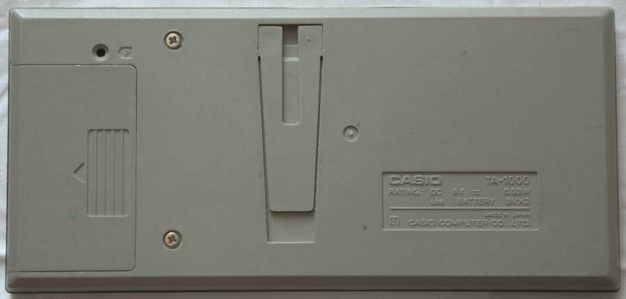
| removal of these screws voids warranty... | ||
 |
||
|
|